Introduction
Transponder is intended for the use in the
Cubesat type satellite P-sat as single board with connection to other parts of
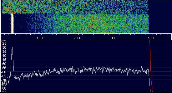
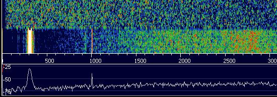
the satellite. Single channel 3kHz bandwidth is intended
for multiple PSK31 transmissions through transponder with FM signal
downlink. Additionally the beacon is
implemented to identify the channel and to give info about transponder health.
Mission status
Transponder
is onboard the cubesat Psat
planned for launch on AFSPC-5 mission on May 20 2015 from
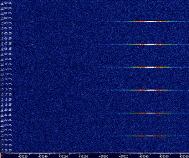
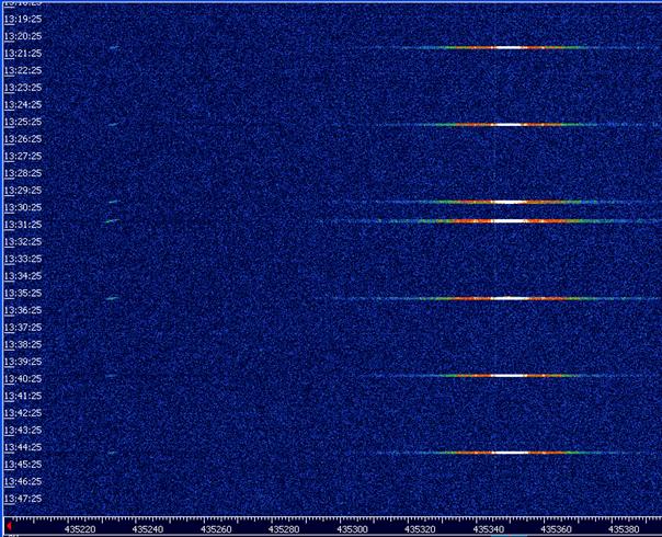
Reception reports
We will be
very grateful for any info about transponder downlink status around the world.
You can send us decoded telemetry frames on our email
psktransponder@centrum.cz. Please specify time of the reception and position of
station. Additional info would be welcomed. If you save the demodulated audio,
send us the wav files, the email should handle great amount of data. If you use
the SDR radio for reception, nondemodulated IF with
bandwidth minimum 40kHz accommodating thermal drift
and doppler would be welcomed.
Function
description
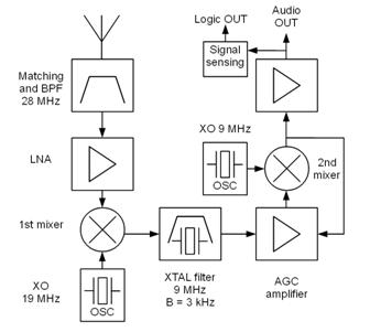
Fig.1
Receiver block diagram
A block
diagram of the HF receiver part of the band monitor is depicted in Fig. 1.
We use a double conversion super heterodyne, proven in PCSAT2 receiver, with
several modifications - especially the BPSK31 signal sensing circuits.
The
receiver includes low noise preamplifier with BFS17 in order to compensate
electrically short receive antenna, which must be shorter to fit in the small
Cubesat. The LNA is followed by high quality LC filter for the out of band
signal suppression. Then there is first mixer NE602 to intermediate frequency
followed by a crystal filter, which defines actual bandwidth 3 kHz of monitored
HF band. The intermediate frequency amplifier A281D with the gain setting
ability for automatic gain control then amplifies the received signal and it is
followed by the last mixer NE602, which converts the signals to the audio band.
The baseband
signal is then splitted into three ways. The first
signal is rectified and the obtained DC voltage controls the gain of the
intermediate amplifier via the MC34072 amplifier.
The second
signal is rectified to get 31.25 Hz frequency from the received signals. Then
it is amplified and filtered by MC34072. This spectral component is a part of
the BPSK31 signal modulation which is most frequently used digital mode in the
monitored radio-amateur band. After passing through the narrow bandwidth tone
decoder NE567, binary signal carrying information about presence of BPSK31
modulation is obtained. It is monitored by a control microprocessor of
transmitter in order to recognize useful signal and switch the power amplifier
on.
The third
signal is also amplified by MC34072 which also works as amplitude limiter and
through preemphasis filter it is connected to the
transmitter modulation input to modulate the UHF carrier.
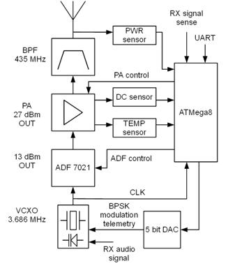
Fig.2
Transmitter block diagram
The
transmitter produces FM modulated signal in UHF frequency band. Output RF power
of the transmitter is 27 dBm at 435 MHz. A BPSK
modulator with data rate 31.25 bit/s on a sub carrier with frequency 312.5 Hz
is implemented in order to transmit telemetry data from built-in sensors. Block
diagram of the transmitter is depicted in Fig. 2.
The core of
the transmitter is integrated transceiver IC ADF7021 produced by Analog
Devices. This solution with minimum number of external components results in
minimal dimensions of the PCB board. The ATMega8 3.686MHz quartz oscillator is
directly modulated by a varicap in order to achieve linear
FM modulation. Output power is amplified by one-stage PA with a Mitsubishi RD02MUS1B
MOSFET transistor. On the board are implemented sensors which measure drain
voltage, current (MAX4372) and temperature (AD7415) of the PA transistor and
also the output RF power (LTC5531) - not used. All sensors and the transceiver
IC are controlled by microcontroller ATmega8. The microcontroller also drives a
5-bit parallel DA converter, which provides BPSK modulation of the telemetry
data.
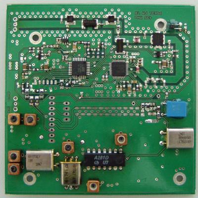
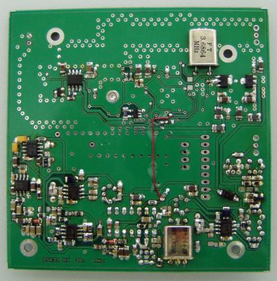
The board
is 1.5mm FR4 material with the size 91.4 mm x 91.4 mm.