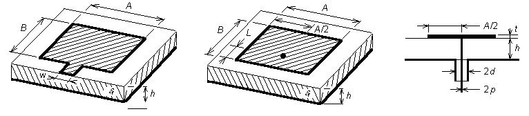
4.4 Microstrip dipoleBasic theoryMicrostrip antennas are frequently used in today's wireless communication systems. Thanks to their low profile, they can be mounted to the walls of buildings, to the fuselages of airplanes or to the reverse sides of mobile phones. Moreover, microstrip antennas are fabricated using the same technology as producing printed circuit boards. Therefore, the fabrication is relatively simple and well reproducible. Finally, microstrip antennas can be simply integrated directly to microwave circuits, which are based on microstrip technology, and therefore, no special transmission lines, symmetrization circuits or connectors are needed on the contrary to classical antennas [8]. Nevertheless, there are several disadvantages of microstrip antennas. Narrow operation band is the main disadvantage. Due to this property, the design of microstrip antenna arrays exhibiting sufficiently low level of side-lobes is a really hard nut to be broken. Even the parasitic radiation of the feeding microstrip network, which can deform the directivity pattern [8]. One of the most frequently used types of microstrip antennas, the patch antenna, is depicted in fig. 4.4A.1a. The antenna consists of a conductive rectangle of the dimensions A × B, which is etched on a dielectric substrate. The antenna is fed by the microstrip transmission line (fig. 4.4A.1, the microstrip goes from the front edge of the substrate crossways from the left). The second side of the substrate (on fig. 4.4A.1a depicted as the bottom one) is continuously electroplated. The electroplated side plays the role of a reflector in the sense of zero potential (from the point of view of feeding) and in the sense of limiting radiation in the direction behind the reflector. Further, we call the electroplated side the ground plane. The microstrip antenna that is fed by the microstrip transmission line (fig. 4.4A.1a) can be considered as an open (non-shielded) open-ended transmission line, which is significantly widened at its end. If electromagnetic wave propagates along such transmission line, electromagnetic energy is primarily radiated into surrounding at the non-homogeneities (spontaneous widening of the microstrip at the border of the feeding line and the antenna element and the open end of this element) of the transmission line. The structure therefore behaves as a transmitting antenna. Moreover, if the length of the microstrip antenna element equals to the half of the wavelength on this widened transmission line, then input impedance of such an antenna is purely real [8]. Then, the antenna is said to be in resonance. Radiation of a microstrip antenna can be explained in different ways. We can come out of the current distribution on the antenna element, which can be consequently understood as a wire antenna consisting of a very wide and a very thin antenna conductor. Next, we can come out from the line of electric intensity at the front side and at the back side of the antenna element (from the point of view of the feeding transmission line) and we can explain the radiation as an effect of a strong horizontal component (i.e. of the component, which is oriented in parallel with the ground plane) of electric field intensity vector at those edges. As an alternative to the microstrip feeding of the microstrip antenna, a feeding by coaxial probe can be used (fig. 4.4A.1b). Whereas the outer conductor of the coaxial cable is connected to the grounding plane, the inner conductor goes through a gap in the grounding plane and continues through the substrate to the microstrip antenna element, where it is fixed (fig. 4.4A.1c). Significant reduction of the parasitic radiation of the feeding transmission line is the main advantage [8].
On the other hand, the coaxial feeding losses the main advantages of the microstrip feeding - a simple realization of a feeding system when microstrip antenna elements are grouped into arrays. Now, turn our attention to the mathematical modeling of microstrip antennas. Thanks to the popularity of microstrip antennas, several types of models of those antennas have been developed. Numerical models are of different validity domains (some are valid for lower microwave frequencies, some are valid for a limited interval of dimensions, etc.). Numerical models significantly differ even in their CPU-time demands (some models are based on closed-form expressions, which leads to low computational requirements, and some models are based on numerical methods, which leads to high CPU-time demands). The methods significantly differ even in the reached accuracy.
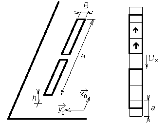
In the next, we concentrate on modeling microstrip antennas by the method of moments, which was described in the paragraph 4.1. As already said, the method comes out of Maxwell equations in the integral form, and therefore, we compute voltages and currents on the microstrip antenna element instead of searching for the distribution of electromagnetic field in the antenna surrounding. In this paragraph, we are going to simplify the analysis. Instead of analyzing a patch antenna, we deal with a microstrip dipole (fig. 4.4A.2) only. At the dipole, a small width of the antenna microstrip B is assumed. Then, only longitudinal currents (direction x) need to be considered and one-dimensional problem is going to be solved, which is an analogy to the solution of a wire dipole (paragraph 4.1) Analyzing the antenna, we assume an infinitely wide substrate, infinitely small thickness of metallic layers t ≈ 0, perfect electric conductivity of all metallic parts, lossless dielectrics and vacuum in the antenna surrounding. Assume a plane wave of an angular frequency ω, which impinges the microstrip dipole. The electric field intensity vector EI (the upper index I denotes the incident wave) describes the incident wave. This wave induces conductive currents in the antenna wire, which are described by the current density vector J. Since the current has to be zero at the ends of the microstrip dipole, a charge described by the charge density ρ is accumulated here. In the following half-wave, the orientation of conductive currents is changed and the accumulated charge leaves the dipole [9]. The effects of currents are described by the vector potential
and the effects of charges are described by the scalar potential
Value of the vector potential A(r) in the observation pint r on the microstrip dipole can be computed by the consecutive addition of contributions of components of the current density vector J from all the points of the microstrip antenna element r0 whereas the current density vector J is multiplied by the respective column of the dyadic Green function GA. The observation point, where the value of the vector potential is computed, is determined by the vector r. Summation of contributions of all the currents flowing on the surface of the antenna element to the vector potential A(r) in the point r is performed by the integral over all the surface of the microstrip dipole S. The source points, where currents contributing to the vector potential to the point r are consecutively determined by the vector r0. The argument of the dyadic Green function r|r0 shows the contribution of the current in r0 the potential in r. Dealing with the computation of the scalar potential, the dyadic Green function GA is replaced by the scalar Green function GV, and instead of the current density vector, the scalar charge density r appears. Except of this, eqn. (4.4A.1b) is identical with eqn. (4.4A.1a). As already said, current density and charge density on the microstrip dipole are mutually associated. Therefore, eqns. (4.4A.1a) and (4.4A.1b) have to be completed by the continuity theorem given by
Eqn. (4.4A.1c) expresses the fact that current flowing from a closed region (see the current divergence as the right-hand side) has to equal to the charge reduction in this region within one second (see time derivative at the left-hand side). If both the vector potential and the scalar one on the microstrip dipole are expressed, then the electric field intensity, which is radiated by the antenna, can be computed
Time derivative of the vector potential jωA describes a dynamic contribution of electric charge on the dipole to the transmitted wave (electric conductive currents, i.e. charges in motion, are sources of vector potential). Gradient scalar potential gives a static contributionof electric charge on the dipole to the transmitted wave (static charges, which are concentrated this moment at the ends of the dipole, are sources of scalar potential). The final problem, which has to be solved, are boundary conditions. Since all the metallic parts of the antenna are perfectly electrically conductive, components of electric field intensity, which are tangential to the antenna surface, have to be zero on this surface
In the above-given relation, ES denotes electric intensity of a wave, which is transmitted by the antenna, and EI is electric intensity of a wave, arriving to the antenna from outside. The vector n0 is unitary vector, which is perpendicular to perfect electrically conductive surfaces. As already explained in the paragraph 4.1, analytical solution of (4.4A.1) is unknown, and therefore, we utilize the moment method for its solution. In the first step of the analysis of the microstrip dipole, the antenna is placed to Cartesian coordinate system (fig. 4.4A.2). Next, vector equations (4.4A.1) are rewritten in the elected coordinate system to the scalar form. Moreover, we assume a special case when moving on the surface of the microstrip dipole (thanks to the boundary conditions, value of the tangential component of electric field intensity is known, which can be used further). We start at eqn. (4.4A.1a), which describes dependency of vector potential on current density vector. The mutual relation between those two quantities is described by dyadic Green function. In a fact, dyadic Green function is a matrix 3 × 3 which elements are functions describing dependency of components x, y, z of vector potential on the components of current density vector. A single scalar element GAst of this dyadic Green function can be understood as s-th component of vector potential, which is supplied by an elementary electric dipole (described by a constant current density vector) in the direction t. Obviously, only the component xx of dyadic Green function is non-zero (assuming a very small width of the microstrip dipole, y-component of current density vector is zero and the only non-zero Jxx can be source of x-component of vector potential Ax; other components of vector A are of zero value). If x component of vector potential (i.e., the component oriented along the dipole) is going to be computed, then (4.4A.1a) can be rewritten to
Here, (xm, yn) are coordinates of a point on the surface of the dipole, where vector potential Ax is computed. Coordinates (x', y') specify the position of x-component of current density, which supplies x-component of vector potential. During the integration, coordinates (x', y') walk through all the points of the antenna surface S. The symbol Jx denotes x-component of current density vector, the symbol Gaxx represents x diagonal term of dyadic Green function. That way, (4.4A.1a) is adopted for the case of the analyzed antenna, and therefore, the attention is turned to the rearrangement of (4.4A.1b). Since (4.4A.1b) is a scalar equation containing scalar quantities only, the adoption consists in considering the introduced coordinated system
Again, scalar potential V is computed on the surface of the dipole in the point (xm, yn). Computing this potential, the product of scalar Green function GV and charge density r is integrated over the whole surface of the dipole. The movement on the surface during integration is done by changing coordinates (x', y'). Next, we turn our attention to continuity equation (4.4A.1c). Since only x-component of current density vector is non-zero (conductive currents can flow in the direction of dipole axis only), the relation can be rewritten to the form
Considering (4.4A.4), charge density r can be expressed as a function of current density Jx and can be substituted to (4.4A.3). That way, charge density is elliminated from (4.4A.3) and both potentials are expressed as functions of components of current density vector
Further, vector potential (4.4A.2) and scalar potential (4.4A.5) are substituted to (4.4A.1d), which enables us to compute electric field intensity of the radiated wave. Since both vector potential (4.4A.2) and scalar one (4.4A.5) are functions of an unknown current distribution on the surface of the dipole, even electric field intensity is a function of this current distribution
Magnitude of electric field intensity on the surface of microstrip dipole can be determined, assuming perfect electric conductivity, from boundary condition (4.4A.1e). Current distribution Jx is the only unknown in (4.4A.6). And the equation (4.4A.6), which contains the unknown function Jx(x, y), is going to be solved by moment method The way of obtaining a piecewise-constant approximation of current distribution on the basis of (4.4A.6) was described in the paragraph 4.1. Therefore, the approach is here reminded only.
The whole algorithm described by the above points is given in detail in the layer B and in [10], [11]. Replacing all the derivatives by central differences in the above-given algorithm, we obtain a matrix equation
In this equation, Ux is column vector of voltages in the direction x on discretization elements. This voltage is computed by multiplying x-component of electric field intensity by x-size of the discretization element
The symbol a denotes the height of the discretization element (i.e. the size in the direction x). Since the microstrip dipole is supposed to be fabricated from perfect electric conductor (voltage on this conductor is zero), the vector of voltages is filled in by zeros only except of elements relating to the excitation gap. Next, Ix is column vector of currents in the direction x, which is unknown this moment for us. Elements of Ix are related to the component of current density Jx as follows
(B is the width of the dipole, and consequently the width of the discretization element). Impedance matrix Zxx describes contribution of currents Ix and contribution of charge densities ρ (expressed from continuity equation (4.4A.4) using x-components of current density Jx on elements) to voltages Ux on those elements. Elements of the impedance matrix Zxx are known (see the layer B)
In order to evaluate the impedance matrix Zxx, values of integrals of Green functions ΓAxx and ΓV over the surface of the discretization element have to be computed for various distances between the source elements (over its surface, current distribution and charge one are integrated) and the observation one (on its surface, electric intensity is computed. Description of the numeric computation of those integrals in Matlab is given in the layer D. Matlab program, which performs analysis of the microstrip dipole by the moment method, is described from user's point of view in the layer C. Here, we provide only illustration results obtained by the program.
For simplicity, the substrate between the dipole and the reflector is assumed to be of the same parameters as vacuum. If the dipole length equals to one half of wavelength and if the dipole width is B = λ/1000, following values of input impedance are obtained (in the first row of the table, the number of discretization elements to which antenna is subdivided is given):
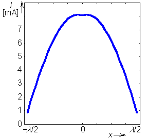
The results show the method to exhibit good stability with respect to the number of discretization elements. Moreover, the input impedance of the microstrip dipole with the reflector computed by moment method, is close to the results of analytical computations (sinusoidal current distribution Jx a wire dipole over an infinite planar reflector assumed). For a single wire dipole, radiation resistance of the antenna (related to the input) equals to RΣ= 85.6 Ω. Investigating approximation of the distribution of x-component of the current along the microstrip dipole, we can show that depicting approximation coefficients from the vector Ix into a chart. That way, we obtain a course which is close to a sinusoidal current distribution (see fig. 4.4A.3). | ||||||||||||||||||||||||||||||||||||||||||||||||||||||||||||||||||||||||||||||||||||||||||||||||