4.5 Microstrip antennaAdvanced theoryIn this paragraph, two-dimensional moment analysis of a patch antenna is presented. In a fact, the approach from par. 4.4 is extended for another dimension. As already said, electric field intensity has to be expressed as a function of currents and charges over cells. For that purpose, vector potential A and scalar potential φ are used. Moreover, the positive convention exp(+jkr) is considered
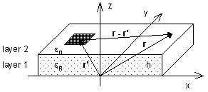
Vector potential A and scalar potential φ of elementary planar currents and charges physically represent contributions of sources to the electric field in a given point. From the mathematical point of view, potentials are the solution of Sommersfeld integrals. For simple situations, potentials can be composed on the basis of the physical point of view. This approach is used even here. Assume a two-dimensional antenna element over the ground plane (fig. 4.5B.1). Relative permittivity of the dielectrics is considered (for this moment) to be one, and contribution of an elementary current facet and charge one in the position r’ to the intensity in r is computed. Using Coulomb (resp. Biot-Savart) low and respecting influence of ground plane (mirror principle), we get
where the distances r0 and r1 are
Here r = (x, y), r’ = (x’, y’) and h denotes the height of the substrate. Including the influence of the dielectrics is more complicated. The physical notion tells us that wave can propagate to the observation point r by the infinite number of paths:
where and εr is relative permittivity of the substrate. Vector potential A stays unchanged. In the case of sources of finite dimension (rectangular cells), the contribution is expressed in integral way
where GA and Gq are Green functions for magnetic potential and electric one, σ is charge density. Now, eqn. (4.5B.2) is discretized. In order to meet this task, a contribution of an arbitrary current (charge) cell to the potential in the center of another cell has to be expressed. Therefore, we denote
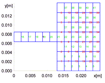
Expression mijAx tells how j-th current cell for x-component contributes to vector potential in the center of i-th cell. Similar meaning is observed at mijAy for Jy and at mijφ for scalar potential. As shown in the layer A, meshes of current cells and charge ones are mutually shifted for one half of a cell, and hence, a different numbering is used. Moreover, we independently number current cells for x-component and y-component. This fact is illustrated by numbering in fig. 4.5B.2, which corresponds to the structure in fig. 4.5A.3.
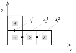
Composing equations for unknown current distribution, we have to know a function describing contributions between two arbitrary cells (of the same type). Due to the limited space, we do not describe this function here. We state only that all the contributions are evaluated at the beginning of the program. Moreover, several contributions repeat (e.g., cells 1 and 2 for the component Jx are of the same contribution as cells 3 and 4). The mutual contributions are stored in a moment table (matrix). Calling the function, a contribution on a respective position of the table is read. Now, the set of equations can be composed. We do not introduce a general relation, but a given simple situation is described. Fig. 4.5B.3 contains a L-shaped antenna element, consisting of four charge cells and three current cells (two of them are related to Jx, one of them to Jy). Next, equations for E1x are built:
The first term represents the contribution of all current cells to the current cell Jx1.The second term represents the contribution of charge cells; expression {}/Δx denotes replacing the derivative ∂φ/∂x by the central difference (see par. 4.1). Brackets contain three terms since there are four charge cells. E.g., the first term represents the contribution of the first charge cell to the center of the second cell minus the contribution of the first charge cell to the center of the first cell. I.e., the first index at m denotes the center of the observation charge cell, where the contribution is computed, and the second index denotes the source cell. Charge in each cell is evaluated using nodal current densities and exploiting continuity equation
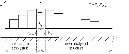
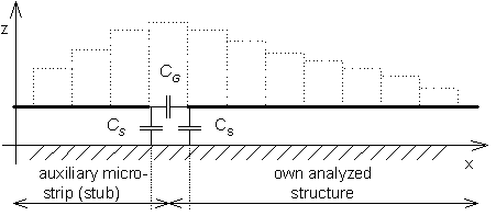
where J[A/m] and σ[C/m2] are current density and charge density. Similarly, equations for E2x and E1y can be composed. Next, we turn our attention to feeding the structure. Plane wave feeding is the simplest way of feeding (see par. 4.4). For each current cell, we substitute Ex = -ExI and Ey = -EyI, where ExI and EyI represent components of incident wave. In our situation, the antenna is assumed to be fed by a voltage source, which is connected between the analyzed structure and an auxiliary microstrip (the incident wave is not considered). In detail, the situation from fig. 4.5B.2 is depicted in fig. 4.5B.4. In the position, where 1 denoted the input port in fig. 4.5B.2, a voltage source of a voltage VS is considered. The source supplies the structure by the current IS. One pole of the source is connected to the analyzed structure, the second pole is connected to the auxiliary microstrip (stub), which represents a certain impedance Zstub related to ground. Input impedance Z1 is then given by the relation
where the impedance ZS is determined as the ratio of the voltage VS (its value is eligible) and the current IS. The impedance Zstub is computed analytically as –Z0cotg(β lstub).
If impedance is computed by the above-described way, the result does not correspond to the reality because influence of edge capacitances is not considered (see fig. 4.5B.5).
Respecting capacitances, the impedance Zstub has to be added in parallel to ZS = 1/jω CS (CS is not open-end capacitance, but it is smaller). That way, we get Zstub’ = Zstub || ZS. Capacitance CG is already included in the impedance ZS and computing impedance Z1‘ = ZS – Zstub‘, we have to subtract ZS. The final impedance is Z1” = Z1‘ ZS / (Zs–Z1‘). Finally, we give a note about feeding the structure. We can assume the structure to be fed by a voltage source connected between the microstrip and ground. This approach causes the direct computation of input impedance from the voltage and the current to provide results, which differ from the measured value. The reason of this difference is hidden in the fact that long cables are used for measuring, and therefore, the TEM wave (forward one, backward one) is present in the point of interest. If feeding is implemented by the above-described source connected between the microstrip and ground (localized feeding), then field distribution at the positive pole does not correspond to the field caused by TEM waves, but end effect influences results. In practical life, the result of localized feeding has to be transformed to the long-cable feeding (vertical de-embedding). The current standing wave has to be de-composed to the forward wave and the backward one. De-composition is not performed at the source port, but is shifted to the right. If both the waves are known, then reflection coefficient can be evaluated at the position of measurement. Then, the phase of reflection coefficient is shifted to the computation position. The set of equations for unknown nodal values was built respecting physical principles. Now, the mathematical approach, which corresponds to the above-described notions, is given:
In the layer C, the patch antenna analysis by the moment method is illustrated by an example. |
