6.1 Analysis of frequency selective surfacesBasic theoryIn this paragraph, reflection coefficient and transmission coefficient are computed for an infinite periodic frequency selective surface. The attention is turned to the surface consisting of rectangular elements (metallic, slot). First, the surface is assumed to be fabricated from such dielectrics, which properties are identical with surrounding. At the end, a brief note on the analysis of real substrates is provided. Numeric analysis of frequency selective surfaces There are two approaches to the analysis of frequency selective surfaces. The first one is based on the method of induced electromotoric forces and enables to analyze surfaces of both the finite extent and the infinite one (in most cases, the method is applied to infinite structures). Analysis by the method of induced electromotoric forces is not described here; readers interested can find more information in [17]. Spectral domain moment method is the second way of analyzing frequency selective surfaces [18]. We concentrate to this method only.
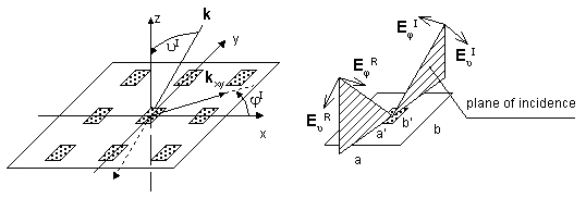
Metallic elements We assume a periodic surface as depicted in fig. 6.1A.1. The surface is illuminated by a plane wave. Projection of wave vector k to the plane of the surface is denoted by kxy. Electric filed intensity of incident wave can be expressed then as follows:
Here, α0, β0 are negative projections of wave vector of incident wave to the directions of coordinate axes x and y (the exponential term exp(+jkr) is assumed for increasing phase in the direction of propagation). Projections of wave vector in the described coordinate system are given as follows:
The symbol E0 denotes electric-field intensity vector in the origin of the coordinate system and k is free-space wave number. In general, the incident wave is of both the parallel polarization and the perpendicular one. If field intensity of the incident wave is expressed in spherical coordinate system (fig. 6.1A.1), then components EϑI and EφI represent directly the parallel component and the perpendicular one. If frequency selective surface is going to be analyzed, components of electric field intensity in the plane xy have to be known. We can evaluate them re-computing EϑI and EφI as follows:
Due to the periodicity of the surface, all the necessary quantities (electric field intensity, current density) in the plane xy can be expressed using Fourier series. Using Fourier expansion, density of electric current J [A/m] on metallic element is expressed:
where
are spatial frequencies. Those spatial frequencies are a spatial analogy to the temporal angular frequency ω, which are used for temporal analysis of signals. The only difference is hidden in the fact that time period T corresponds to spatial periods a and b. Coefficients of Fourier series can be obtained by integrating current densities over the whole surface of a cell (inverse Fourier transform)
In analogy to current density, Fourier series can express arbitrary periodic quantity. We do that in the next part, where a plane wave excitation of a selective surface is expressed in the spectral domain (i.e., in the domain of spatial frequencies). Determination of reflective properties of the selective surface is the aim of the computation. Problem formulation
Assume a plane wave falling to a frequency selective surface under angles (ϑ, φ). This wave excites currents in metallic elements, which form a scattered field ES. Whereas the magnitude (not the phase) of the intensity of incident wave EI is constant over the whole elementary cell, the magnitude of the intensity of the scattered wave ES is different in the different points of the cell. Relation between ES and EI changes according to the surface impedance in a given point. For the surface of conductive elements, we get
Here, γ [S.m-1] is electric conductivity of elements. Assuming the electric conductivity of metallic elements to be perfect, the right-hand side of (6.1A.6) approaches zero, and we get
Intensity of scattered electric field ES in a point determined by the position vector r can be evaluated from vector potential A
As a source of vector potential A, currents J induced by incident wave to metallic elements of selective surface can be considered. Contribution of current in r' to the potential in r is described by Green function G. For vector potential, we get
In free space, Green function G is of the form
Combining relations (6.1A.9), (6.1A.8) and (6.1A.7), integral equation for space-domain electric field is obtained:
Eqn. (6.1A.11) is solved in the domain of spatial frequencies. Eqn. (6.1A.11) is mapped to the spectral domain within two steps. First, eqn. (6.1A.8) is mapped by its rewriting to the component form and by expressing vector potential by Fourier series. That way, we get [19]
In the second step, the relation is mapped to the domain of spatial frequencies (6.1A.9) [19]
Evaluating Fourier transform of the function (6.1A.10), we get [19] Green function in spectral domain
where the square-root of negative imaginary part is assumed only. Combining (6.1A.13), (6.1A.14) and (6.1A.12), the final relation for electric field in spectral domain is obtained
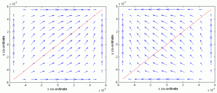
Problem solution Solving the problem, an unknown current distribution in (6.1A.15) is approximated by the linear combination of properly chosen basis functions and unknown approximation coefficients. Such formal approximation is substituted into the solved eqn. (6.1A.15). Since the approximation of the solution does not meet the initial relation exactly, we respect this fact by introducing a residual function (residuum). Lower the residuum is, more accurate the approximation is. The residuum is minimized by Galerkin method (residuum is sequentially multiplied by as many basis functions as many unknown approximation coefficients is computed; that way, N linear algebraic equations for N unknown approximation coefficients is obtained). There are two approaches for choosing basis functions. The first one exploits basis functions, which are non-zero over the whole analyzed area. Functions are elected to physically represent standing waves of a current on an element. The second approach divides the analyzed region to sub-regions, where current is approximated in terms of basis functions, which functional value is non-zero over a given sub-region only. This approach is advantageous in simple analysis of selective surfaces consisting of arbitrarily shaped elements. Here, we concentrate on the first group of basis functions only. As basis functions, harmonic functions are used (first approach, the layer B), and a combination of harmonic functions and Chebyshev polynomials is exploited (second approach, the layer B). A more detailed description of the above-given basis functions for solving (6.1A.15) is introduced in the layer B. Here, obtained results are presented only. Harmonic basis functions Assume a frequency selective surface consisting of rectangular perfectly conductive elements of the dimensions a' and b'. If current distribution over an element is approximated in terms of harmonic basis functions, we obtain for the mode (1, 1) for the parallel polarization such current distribution, which is depicted in fig. 6.1A.3a, and for the perpendicular polarization, the distribution from fig. 6.1A.3b is obtained
Combination of harmonic functions and Chebyshev polynomials
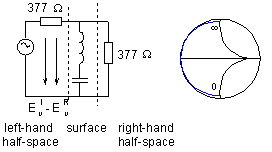
In contrast to purely harmonic basis functions, the function cosine is replaced by Chebyshev polynomial, which is of infinite magnitude at the edges of the element. That way, strong currents flowing along edges are correctly modeled. An equivalent circuit can describe behavior of frequency selective surfaces, which consist of metallic elements, where inductances of elements together with capacitances among ends of elements create a serial resonant circuit (fig. 6.1A.4). Reflection coefficient r (see fig. 6.1A.4) is evaluated according to
Here, PI is power of incident wave and PT denotes power of wave, which was transmitted by the surface to the right-hand half-space. Resistance 377 Ω models free space in front of the surface (left) and behind the surface (right).
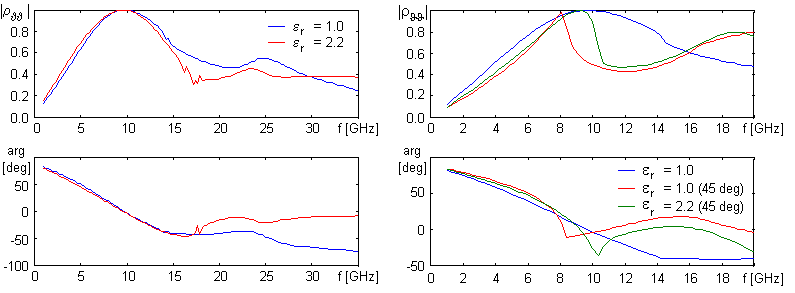
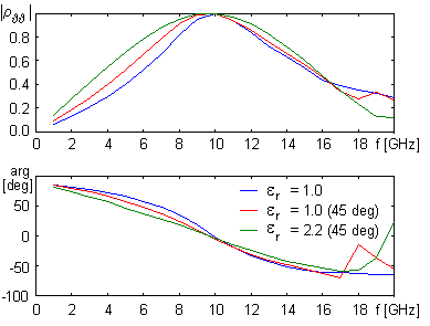
Frequency course of reflection coefficient of the surface for parallel polarization is depicted in fig. 6.1A.5. Considering the surface without dielectrics, (b = 21 mm, a = 7.5 mm, b' = 19.75 mm, a' = 1.5 mm), there is a break of the steepness of the reflection coefficient course around 14.3 GHz; this phenomenon is caused by the excitation of the first parasitic mode (grating lobe). Adding dielectrics and modifying dimensions (b = 17 mm, a = 7.5 mm, b' = 15.75 mm, a' = 1.5 mm, height of the substrate d = 1.57 mm) causes a small decrease of the selectivity on one hand, but the stability of tuning for un-normal incidence is increased on the other hand (see fig. 6.1A.5b). Further increase of the stability of reflection coefficient with respect to the angle of incidence can be reached by adding an upper dielectric layer. Thanks to the dielectrics, cell dimensions are smaller and parasitic modes are excited at higher frequencies (17.6 GHz). In fig. 6.1A.5b, no significant effect of this mode can be observed. Both the normal incidence and the un-normal one excite parasitic resonance at higher frequencies. At frequencies, which are higher than the frequency of the first parasitic mode, the course of reflection coefficient does not express the total intensity of the reflected wave, but only the intensity of the basic mode (0,0). Considering perpendicular polarization of incident wave (in contrast to parallel one), reflection coefficient is nearly independent on the angle of incidence (see fig. 6.1A.6). If a surface without dielectrics is considered, dimensions b = 21 mm, a = 7.5 mm, b' = 19.75 mm, a' = 1.5 mm, are assumed., If dielectrics is considered, dimensions b = 17 mm, a = 7.5 mm, b' = 15.75 mm, a' = 1.5 mm and the height of the substrate d = 1.57 mm are assumed.
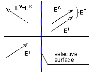
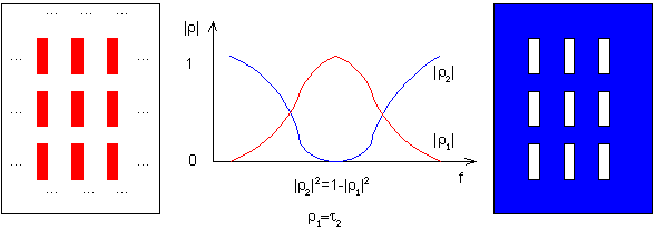
Slot elements In contrast to the surfaces of metallic elements, frequency selective surfaces of slots exhibit an opposite dependency of reflection coefficient, i.e. they behave as a band-stop filter. If no dielectrics and a single metallic layer are assumed, then slot surfaces are true complements of metallic-element surfaces.
Now, we turn our attention to the derivation of equations for magnetic intensity over the aperture of slot surface in spectral domain. Considering the case without dielectrics and with a single metallic layer, duality principle can be applied: in (6.1A.15), we exchange E with H, ε with μ, J with JM
Comparing (6.1A.17) and (6.1A.15), a certain inconsistency can be revealed: coefficient 2 appeared at magnetic current density and exciting magnetic intensity. Next to the duality principle, the following fact had to be considered: Field radiated by electric currents of the metallic-element surface is not scattered by those elements, whereas magnetic currents in slots produce a field, which is scattered by the conductive plane [19]. In order to include the influence of the surrounding of the conductive plane, following steps have to be done:
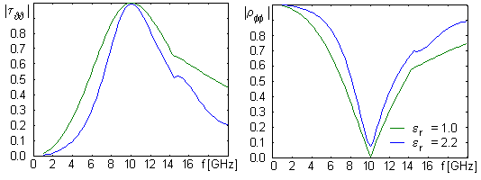
In analogy to metallic elements, dual formulation of transmission coefficient is possible τ. In fig. 6.1A.9, an example for normal incidence of a wave to a frequency selective surface with slots in vacuum (b = 21 mm, a = 7.5 mm, b' = 19.75 mm, a' = 1.5 mm) and on dielectric substrate (b = 14 mm, a = 7.5 mm, b' = 13.25 mm, a' = 1.5 mm and the height of the substrate d = 1.57 mm) are given. Obviously, selectivity of transmission coefficient is better for dielectrics (in case of metallic-element surface, the situation was opposite). Next, influence of dielectrics is different compared to metallic-element surface, and therefore, slots are of different dimensions compared to metallic-element surface with dielectrics. Dielectrics even cause non-zero value of reflection coefficient on resonant frequency. Even here, parasitic modes appear. Conclusion The method of the analysis of frequency selective surfaces, given in this chapter, does not include the influence of dielectrics, but given examples do that [17]. Another way of the description of the influence of dielectrics can be found in [19]. Real applications use several sequentially lined selective surfaces. That way, selectivity can be significantly improved. Design of such surfaces is rather complicated. Frequency selective surfaces can be modeled in commercial programs based on finite elements (HFSS) or on moment method (IE3D). In both cases, only a single element is analyzed thanks to the periodicity. Designing frequency selective surfaces, physical basis of their behavior and limitations have to be known.
| ||||||||||||||||||||||||||||||||||||||||||||||||||||||||||||||||||||||||||||||||||||||||||||||||||||||||||||||||||||